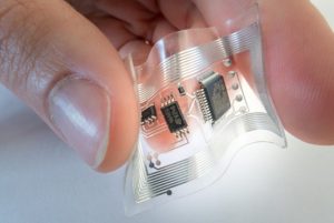
The manufacture of autonomous, ultra-thin, flexible and conformable devices spread our research from nanomaterials, energy management to heterogeneous integration onto flexible / stretchable substrates. We are active in applications such as: smart interfaces (human machine interface), IoT, micro batteries, smart sensing, bio robotics / mimetic, printing…
In short, we develop and study electronic devices on unconventional substrates ⇒ flexible and stretchable. The goal is to build the electronics of the future that will be foldable and conformable.
 Circuit onto PDMS | 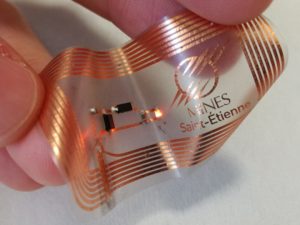 Circuit onto Pa-C |
In particular, optimization of the physicochemical and mechanical parameters which govern their implementation, as well as the realization of models and test procedures to guarantee their functioning and their lifespan are the our main development themes.
The activities of the department are organized within the 660m2-area ‘MicroPackS’ technological platform, in close collaboration with industry. This technological platform contains facilities and technological equipment for R&D activities involving micropackaging, and micro and nano-electronics, in a clean room comprised of a 220m² 1000-class and 400m² 10000-class. The department members have full access to this clean room. It is well-equipped for thin film processing by i) vacuum sublimation, and ii) solution and inkjet printing deposition techniques. Electrical characterization is realized through the use of an automatic probe station and multiple testers. Scanning electron microscopy, Atomic Force Microscopy, X-rays, nanoindentation, Raman spectroscopy and acoustic scanning microscopy will be employed to complete the analysis and device characterization.